
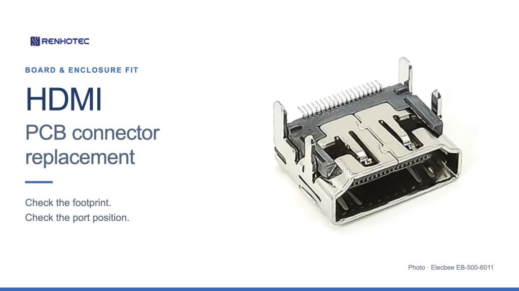
A replacement HDMI socket may accept the original cable yet miss the board’s solder pads, put its fixing legs over copper, or sit too low in the enclosure opening. Before choosing a part, compare the PCB attachment and the position of the mating face with the original assembly.
“HDMI female,” “19 positions” and “SMT” can narrow a search. They do not define a complete footprint. Start with the original part number and drawing revision, if available. When those are missing, document the board and connector before deciding which candidate deserves a sample.
Record the connector from three directions
Take a front view of the mating opening, a side view with the PCB edge visible, and a view of the attachment side. Keep the camera square to the surface you are recording. Include a scale for identification, but use measurements and drawings for the final fit check; perspective can make the near side look wider than the far side.
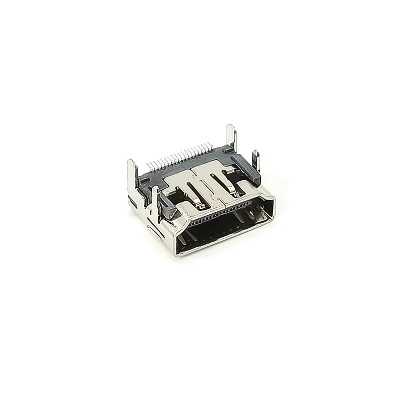
The front view helps identify the interface and its orientation. The side view shows how the connector sits relative to the board and panel. The attachment view reveals the arrangement that a replacement must reproduce: contact tails, shell legs, locating features and any board cut-out.
 AB
A · Contact tails
The fine terminals must align with the intended board connections.
B · Shell legs
The larger metal attachments have their own positions and shapes.
Photo: Elecbee EB-500-6011. Use the selected part drawing for dimensions and contact assignments.
Do not count shell attachments as signal contacts, or infer a contact number from this oblique photograph. Photograph any marking on the old part, but treat an unidentified stamp as a clue rather than a confirmed manufacturer part number.
Separate mounting position from solder attachment
Three descriptions answer different questions. Right-angle or vertical describes the mating direction relative to the PCB. Top or mid mount describes the body’s position relative to the board. Surface mount or through hole describes how specified terminals attach. Read the contact and shell details separately, even when a catalogue offers only one mounting filter.
Above the board
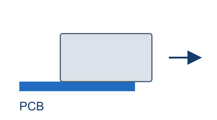
The drawing must locate the mating face and its height from the PCB surface.
Through the board plane
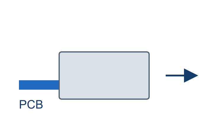
Check the cut-out, board thickness and clearance above and below the PCB.
For a documented top-mount example, TE 2-1747981-1 is listed as right-angle, top-mount and surface-mount. Those are separate fields. A part with the same mating interface but a different board position is a different mechanical candidate.
Read the drawing when the terminology is ambiguous. Same Sky’s HD09-19-MSMT-TR is catalogued as mid-surface mount, while its recommended PCB layout explicitly shows circular contact holes and a board cut-out. The mounting label alone is not enough to create a land pattern or select a solder process.
Compare the footprint before comparing the housing
Use the board drawing and the candidate’s recommended PCB layout at the same units and scale. Establish a common origin, such as the connector centerline and the specified board-edge datum. Align those references first; dragging two outlines until they look close can hide a shift in the contact row.
Next, check the viewing direction and the marked contact numbers. A bottom view of the component and a top view of the PCB can appear reversed. Follow the stated view and numbered endpoints; do not mirror a layout merely to make it resemble a photograph.
| Drawing example | Contact layout | Other features to carry into the comparison |
|---|---|---|
| EDAC 690-019-598T312 Issue 3, PCB layout |
One row of contact pads; 0.50 mm pitch; 9.00 mm end-to-end center span. | Four shell mounting slots and an explicit PCB-edge reference. |
| Same Sky HD09-19-MSMT-TR 2024-09-12, page 3 |
Two staggered rows of Ø0.55 mm contact holes; 1.00 mm pitch within a row and 0.50 mm horizontal stagger. | Board cut-out, shell slots and a specified 1.60 mm PCB thickness. |
These are drawing-reading examples, not alternatives certified to fit the same board. Neither drawing specifies the Elecbee photograph or the Renhotec component discussed below.
Check every attachment feature, not just one confirming dimension. Record pad width and length, hole or slot size, center locations, plating requirements where specified, and the permitted tolerances. A caliper reading across a group of bent tails is useful for screening; it is not a substitute for the recommended land pattern.
Check the port position with the enclosure installed
A footprint can match while the cable still fails to seat. Compare the mating-face position along the insertion direction, its height above a common enclosure datum, and the space around the plug body. Include the panel thickness, any recess and the actual cable’s overmold. The metal plug tip fitting through the opening does not prove that the larger plug housing can reach its seated position.
For the height check, use the reference named by each drawing. A dimension measured from the PCB top surface cannot be added as though it started at the board underside. Mid-mount parts need particular care because the body can extend below the board plane.
This stack is a worked example, not a dimension set for any product shown or linked here.
The nominal connector center is 8.0 + 1.6 + 3.0 = 12.6 mm above the enclosure datum. Adding the stated tolerances gives a worst-case range of 12.2–13.0 mm. If the panel-opening center is 12.6 ± 0.2 mm, the largest relative center offset is 0.6 mm, even though the nominal centers agree.
Suppose the opening’s minimum height is 6.0 mm and the required insertion envelope’s maximum height is 5.0 mm. The nominally centered allowance is (6.0 − 5.0) ÷ 2 = 0.5 mm on each side. A possible 0.6 mm offset exceeds that allowance. This simplified vertical check therefore fails; it does not justify approving the opening from nominal dimensions alone. A complete check must also cover width, corners, insertion depth and the cable’s required bend space.
Keep the component record separate from the assembly decision
Renhotec RHT-692-2002 is listed as a female HDMI connector for PCB/SMT mounting. That identifies a component to discuss when the design calls for that interface and attachment method. To approve it as a replacement, obtain its exact drawing and compare the board and enclosure dimensions described above.
Compare component candidates in the Renhotec HDMI connector range. Keep the chosen public part number with the requirement sheet so that a drawing, sample and quotation refer to the same component. A drawing for another HDMI socket cannot qualify this part.
Keep the device requirements in a separate column: required video modes, audio or control functions, operating conditions and the tests needed after assembly. A familiar HDMI opening, an SMT label or a mechanical fit does not establish the finished equipment’s supported functions. Replacing a bare socket does not by itself upgrade the device.
Resolve mismatches before ordering the replacement
| Finding | Next action |
|---|---|
| Same opening; different pad or hole pattern | Reject it as a direct replacement for that board. A board redesign is a separate task. |
| Footprint matches; port height or projection differs | Check the complete panel and plug stack before accepting a sample. |
| Only a front photograph is available | Request an attachment-side view and the exact mechanical drawing. Keep the candidate unqualified. |
| Pads are lifted, holes damaged or the board edge is broken | Assess the PCB damage separately. Finding the correct connector does not establish that the board can be repaired. |
| Catalogue and drawing disagree | Ask the supplier to confirm the exact ordering code and controlling drawing revision before approval. |
Record revision changes rather than assuming every change means a new footprint. EDAC’s 2021 engineering change notice for 690-019-598T312, for example, explicitly describes its change as a drop-in replacement with unchanged dimensions, form, fit and function. That statement applies to the named revision change; it is not permission to substitute an unrelated connector.
A useful replacement request includes the old part number or markings, board revision, front/side/attachment photographs, measured PCB thickness, footprint and panel drawing, candidate ordering code, and the required assembly tests. Identify any unavailable item. With those references, the supplier can answer a specific fit question instead of trying to choose a socket from its front face alone.